量子点发光二极管(QLED)在显示和照明领域展现出广阔的应用前景。尤其是氧化锌纳米颗粒(ZnO NP)作为电子传输层(ETL)在器件中的引入,极大的提高了QLED的性能,包括效率、亮度及工作寿命。然而,ZnO在QLED的商业化应用中面临许多挑战。其中最为关键的挑战来自于所谓的“正老化”效应。“正老化”效应是指QLED器件在制备完成后,经过一定时间存放或低电压驱动,器件效率不断上升最终趋稳的现象。这种“正老化”效应积极的一面是使得QLED器件获得最佳的性能,消极的一面是其不可控性。这种不可控性使得QLED阵列难以获得一致的器件性能。目前,QLED的这一“正老化”效应的物理机制尚未明确。
近日,吉林大学物理学院纪文宇、张汉壮教授联合电子学院谢文法教授和刘士浩副教授等人,系统研究了老化过程中酸及金属对ZnO NPs薄膜形貌及光电特性的影响,通过系列原位表征,揭示了基于ZnO纳米粒子薄膜的杂化QLED器件正老化效应的机制。研究发现,酸的作用是诱导了ZnO NP的原位重结晶过程。具体来说,在酸的作用下,ZnO NP发生原位融合(再结晶),此种融合是沿着氧化锌晶体c轴方向,最终形成长程的ZnO晶体,并且粒子的缺陷得到一定程度的钝化。活性金属离子(如Al和Ag离子)从阴极到ZnO中的扩散对ZnO的再结晶起到促进作用,同时进一步钝化了ZnO粒子中的缺陷。最终,重结晶后的ZnO NP薄膜的载流子浓度得到了降低,而电子迁移率得到了极大提高。高的电子迁移率保证了高效的电子注入,而低的载流子浓度抑制了载流子对量子点中激子的猝灭作用。此外,ZnO的陷阱态被钝化,也显著抑制了其对激子的猝灭作用。最终,基于ZnO NP的红色QLED的外量子效率(EQE)从17.2%提升至33.7%。这一结果为QLED电子传输层的优化设计提供了指导。相关结果发表在Light: Science & Applications 期刊上。
论文链接:
https://www.nature.com/articles/s41377-025-01867-1
文章亮点总结:
1. ZnO NP薄膜的电子传输特性随老化过程的演化:正老化过程中,ZnO NP薄膜的电子迁移率显著增强,而载流子浓度降低。这归因于薄膜晶体质量的提高。
2. ZnO NP重结晶现象:酸处理和金属扩散的协同作用下,ZnO NP薄膜发生原位重结晶,ZnO NP沿着c轴方向生长。重结晶过程使得薄膜陷阱显著降低,迁移率大大提高。
3. 正老化机制:正老化的核心机制在于酸处理诱导的ZnO NP重结晶过程,使得ZnO薄膜的电子迁移率大大提高,从而确保电子高效注入;陷阱态得到钝化,载流子浓度降低,抑制了缺陷及载流子引起的激子猝灭效应,使得器件效率得到提高。
4. 器件性能突破:通过正老化,基于ZnO的QLED器件性能显著提升,外量子效率从老化前的17.2%提升至33.7%,约提升了1.96倍。
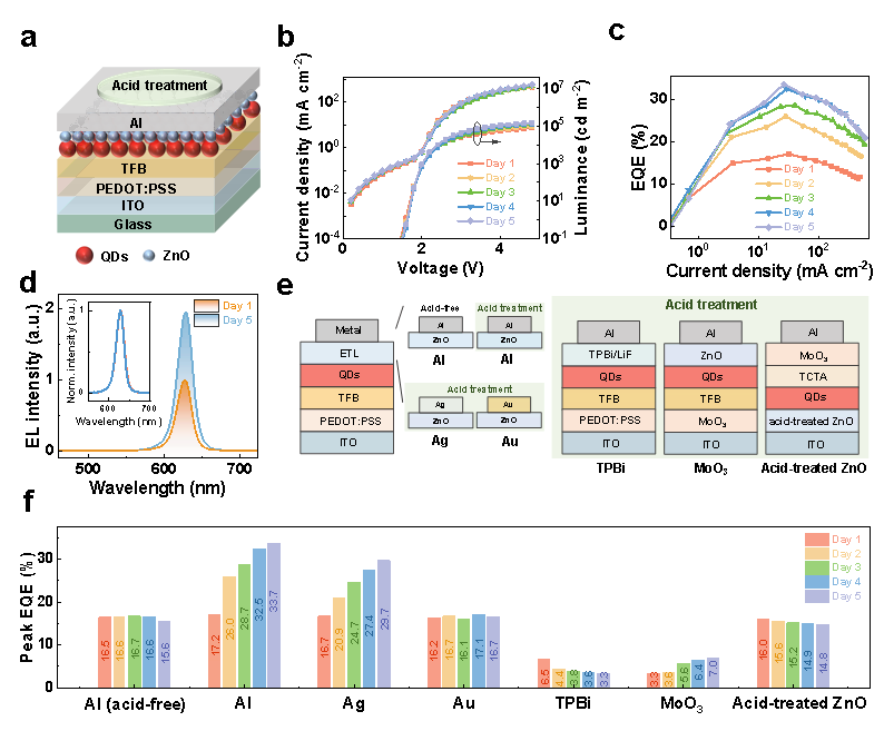
Fig. 1 | Positive-ageing effect of QLEDs. a, Device structure of the red QLED. b, J-V-L and c, EQE-J characteristics of the aged device stored for 1–5 days. d, EL spectra of the device before and after aging, driven at 3 V. The insert depicts the normalized EL spectra. e, Schematic diagram of ZnO-based QLEDs with different metal cathodes (Al, Ag, and Au), labeled as devices Al (acid-free), Al, Ag, and Au, respectively; TPBi-based QLEDs, labeled as device TPBi; MoO3-based QLEDs, labeled as device MoO3; and inverted QLEDs with acid-treated ZnO, labeled as device acid-treated ZnO. f, EQE variation of these devices during storage ageing.
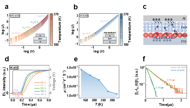
Fig. 2 | Electron transport properties of the ZnO NP films. a-b, J-V characteristics of Al/ZnO/Al devices (a) without acid treatment and (b) with acid treatment at different temperatures. The symbols represent the experimental results, with colors corresponding to the measurement temperatures. c, A schematic diagram of the device structure ITO/QDs/ZnO/Al and its working mechanism for measuring electron mobility in ZnO. d, TrEL spectra of ITO/QD/ZnO/Al devices at different temperatures. e, Temperature-dependent mobility of a ZnO film with acid treatment. f, Plot of  as a function of time, with the green line representing the fitted curve.
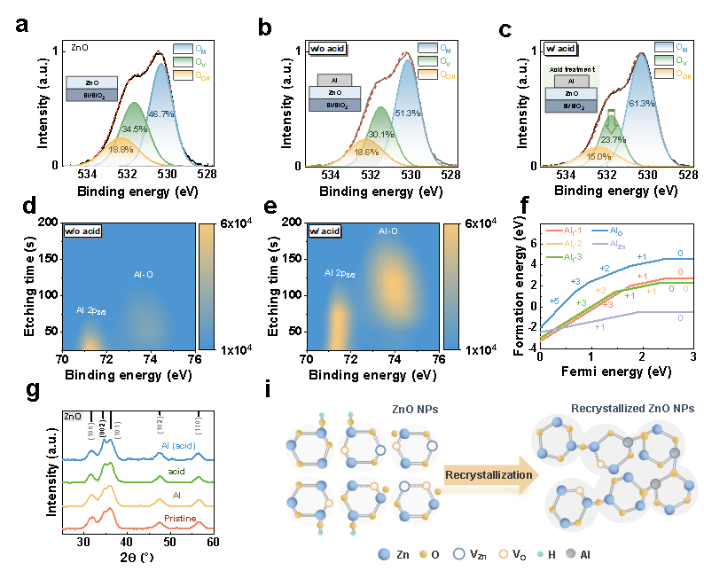
Fig. 3 | Operando chemical reactions of ZnO NPs. a-c, Deconvolution of the O 1 s XPS peaks of the (a) pristine ZnO film. (b) Al-deposited ZnO film without acid treatment and (c) Al-deposited ZnO film with acid treatment. d-e Evolution of the Al 2p XPS peaks of the Al-deposited ZnO films (d) without acid treatment and (e) with acid treatment as a function of the Ar ion etching time. f, Formation energies of various defects in ZnO films with Al doping. g, XRD patterns of four ZnO samples: pristine ZnO, Al-deposited ZnO film (Al), ZnO film with acid treatment (acid), and Al-deposited ZnO film with acid treatment (Al (acid)). i, Schematic illustration of the recrystallization process of ZnO nanoparticles.
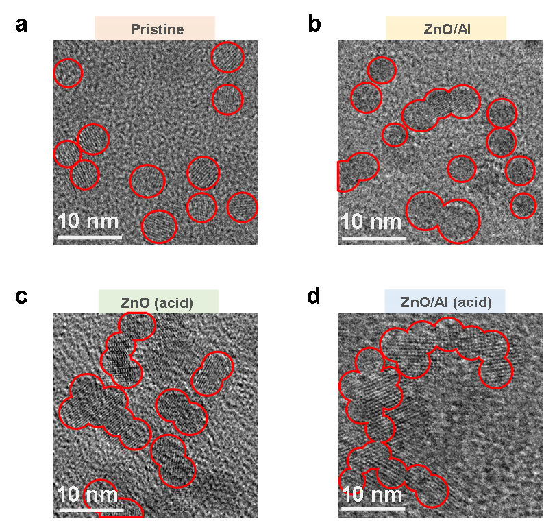
Fig. 4 | Morphology of the ZnO NPs. a-d, TEM images of (a) pristine ZnO, (b) Al-deposited ZnO, (c) ZnO with acid treatment, and (d) Al-deposited ZnO with acid treatment.
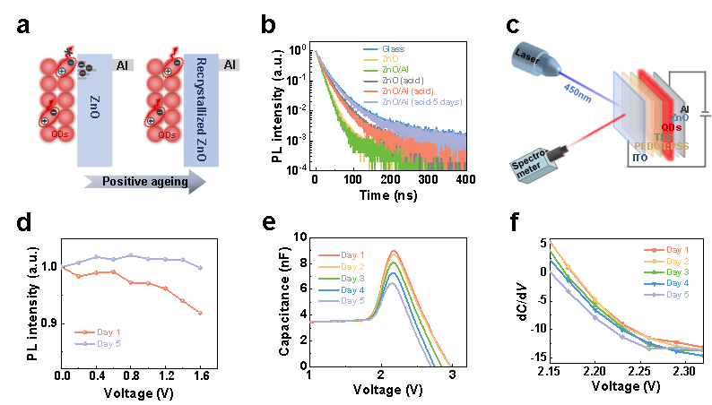
Fig. 5 | Charge–carrier dynamics in the QDs. a, Schematic illustration depicting exciton quenching of QDs by ZnO before and after recrystallization. b, PL decay curves measured for the QDs under different conditions: QDs on glass, denoted as glass; glass/QDs/ZnO, denoted as ZnO; glass/QDs/ZnO/Al, denoted as ZnO/Al; glass/QDs/ZnO with acid treatment, denoted as ZnO (acid); glass/QDs/ZnO/Al with acid treatment, denoted as ZnO/Al (acid); and glass/QDs/ZnO/Al with acid treatment after 5 days of aging, denoted as ZnO/Al (acid-5 days). c, Schematic diagram of the setup for PL spectra testing at a voltage below the turn-on voltage for electroluminescence. d, PL intensity versus voltage curves of the device before and after aging. e, Capacitance‒voltage curves of the device during positive aging, and f, the derivative of capacitance (dC/dV) as a function of voltage (V) during positive aging.
吉林大学物理学院博士生王淞和电子学院刘士浩为本文的共同第一作者,本文通讯作者为吉林大学物理学院张汉壮教授、纪文宇教授、电子学院谢文法教授。该工作得到了国家自然科学基金项目的资助和吉林省科技厅项目的支持。